


Stop Heating the Air: A Smarter Way to Process Wafers
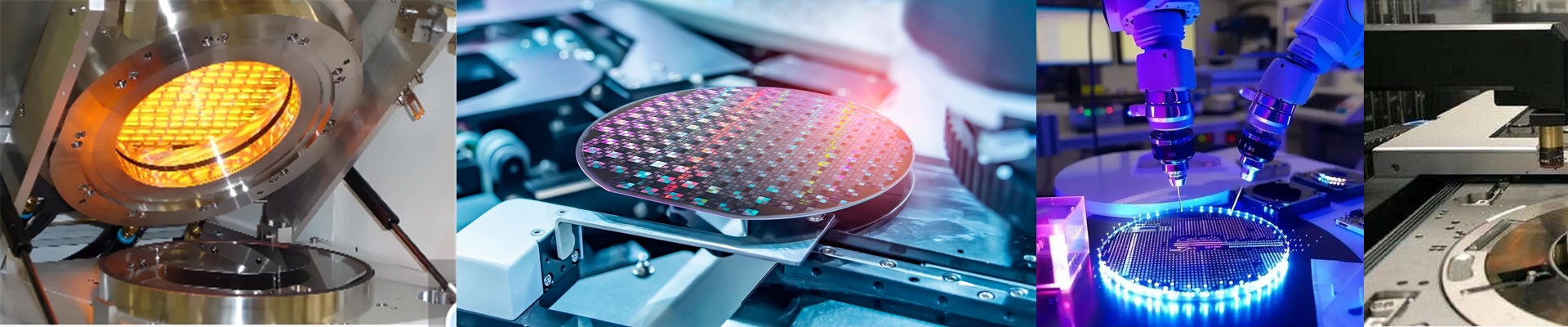
If we’re actually going to hit those carbon neutrality goals in the fab, we have to stop relying on those old-school resistive ovens. They’re energy hogs. Instead, we’re moving toward precision IR heating. The idea is simple: why heat the entire vacuum chamber or the air around the wafer when you only need the wafer itself to be hot? We use IR sensors and lamps to put the heat exactly where it belongs. No more wasting power on empty space.
How it actually works
Standard heating relies on convection. It’s slow, clunky, and uses a ton of juice. IR is different. It uses electromagnetic radiation to move energy. By matching the lamp’s emission to what the silicon actually absorbs, the heat goes straight into the substrate. It’s fast. Really fast. And because the ramp-up time is so much shorter, your total kilowatt-hours per wafer drop significantly.
Keeping it under control
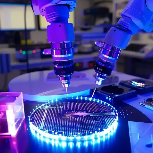
You can’t just blast heat and hope for the best. You need a tight grip on the temperature. We use high-speed IR sensors that watch the wafer surface in real-time. These sensors talk to a PID loop that tweaks the lamp power on the fly. If a hotspot pops up, the system kills the wattage instantly. It saves the wafer from becoming scrap and keeps the power bill down.
The catch (because there’s always one)
Here’s the thing: when you switch to high-density IR lamps, you’re putting a lot of thermal stress on your chassis. Sure, the wafer gets hot quickly, but the surrounding gear takes a beating. You’ve got to make sure your cooling manifolds are beefy enough to handle that concentrated radiant heat. If your cooling loop is weak, you’ll just trade your energy savings for a broken machine.
What this means for the floor
Swapping out those old heating banks for IR arrays makes the curing and annealing stages way leaner. For a lot of legacy lines, it’s a pretty straightforward swap. We’ve noticed a clear pattern: the better the IR sensor, the lower the electricity overhead. It’s a win-win. Less waste, fewer rejected wafers, and a much smaller carbon footprint.