
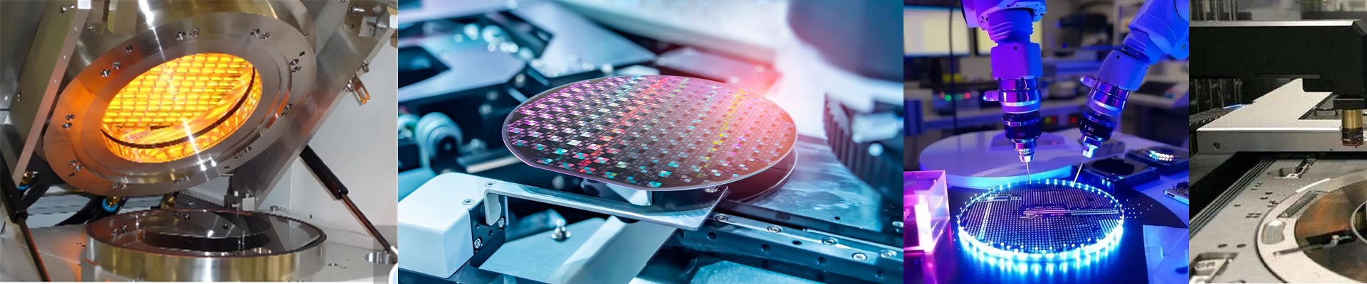



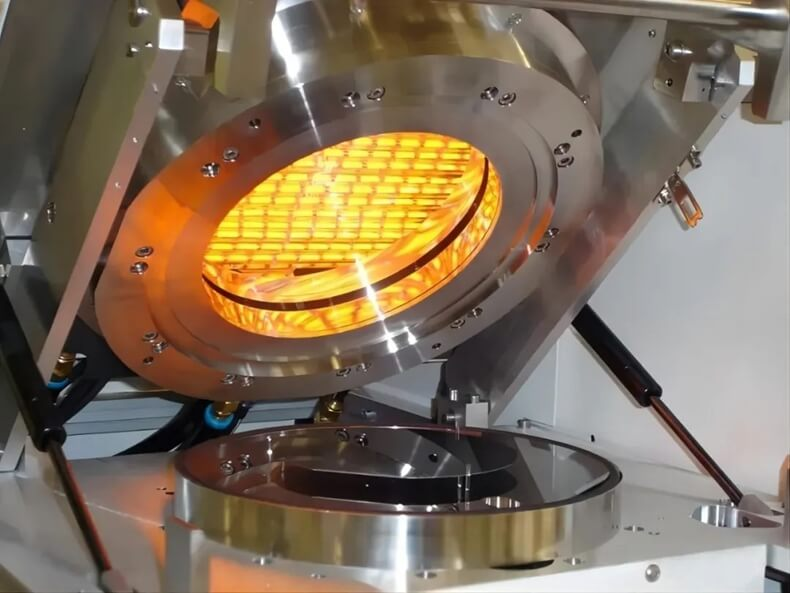
Out on the fab floor, the probe card is under the scope, waiting to run the next lot. If the wafer temperature drifts even a fraction of a degree, your parametric window slams shut and yield starts slipping away. We built this wafer probe heater to stop that drift at the source—right where the probe touches down. What actually matters under test The unit uses short-wave infrared elements feeding a quartz thermal path, tuned for snap response and low thermal inertia. Across the chuck, wafer-level uniformity holds within ±0.1°C, and run-to-run repeatability stays tight because the control loop is closed at the workpiece, not at the heater body. The design drops into standard probe stations and handlers, and the hot zone is isolated so stage motion doesn’t stir up particles. It lives in Cleanroom Class 1–100 thanks to sealed materials and airflow that stays out of the test environment. Why it holds up in production This probe heater was engineered as an equivalent thermal module to international semiconductor equipment, and it’s validated against the same acceptance criteria. In qualification cells, it runs 24/7 with no unplanned downtime tied to temperature excursions. When you’re checking photoresist, it keeps soft bake and hard bake temperatures with a tight distribution, so critical dimension control doesn’t get hammered by thermal nonuniformity. The payoff: fewer retries, stable parametric bins, and lower energy use because ramp-and-soak cycles are shorter. A few practical notes Installation is straightforward, but the heater needs a dedicated, filtered supply to keep cleanroom air quality in spec and prevent coating degradation over time. Matching the mechanical interface and connector pinout to your station is a must for plug-and-run deployment. Once it’s aligned, it runs as a drop-in replacement—no rewriting your process recipe.